3D NAND – When the Only Way to Go is Up
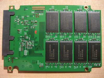
In the past few years, we’ve seen the invention and development of a technology known as 3D NAND. If you’re not sure what NAND is referring to, it’s the type of flash memory used in USB’s, solid state drives, and most other flash memory devices. For more information on NAND flash, watch our video on SSDs. The section on NAND runs from 1:00 to 2:25.
3D Does Not Mean There is a 2D
From a physics standpoint, 3D NAND obviously has as many dimensions as planar NAND. Atoms are 3D, so planar NAND certainly is too. What this new third dimension actually refers to is that the bit lines have been turned on their sides and are instead built straight up, rather than attempting to decrease the die size below 15nm (nanometers) to pack more data in on the x-y plane parallel to the ground.
The comparison often used is to imagine a neighborhood with a bunch of houses. Over the years, these houses have become smaller and closer together to accommodate more residents (more data). Due to the laws of physics, there is a barrier to how small and close together we can make these houses. In order to overcome this, we’ve simply decided to turn the houses into skyscrapers by building straight up.
The process of creating 3D NAND is certainly different than that, but it’s a good comparison for understanding the fundamental difference between the two types.

Process
In order to produce NAND that can be structured vertically, they have to alter a number of design components. Whereas planar NAND just has lines of memory cells next to each other on the same level, 3D NAND takes these same lines, forms them into a u-shape so the cells are on the outside of the “u” extending upwards, and fits multiple of these u’s within the same area that just one line of planar NAND would typically take up.
Samsung also produces their own kind of 3D NAND known as 3D V-NAND, which uses charge-trap technology and storage tubes to create the 3D structure. Each component of the floating gate transistor is turned into concentric layers within a single tube, extending upwards to form vertical memory cells. However, instead of storing electrons within the floating gate, they substitute in an insulator to trap electrons in place of the floating gate.
So Why is 3D Better than 2D?
These 3D NAND technologies have numerous benefits. First off, they lower the cost per bit of the memory, allowing for cheaper flash memory devices at the same storage levels offered today. Following this logic, it also allows for flash memory devices with greater storage capacities, such as the 15TB SSD we’ve been hearing about recently.
Charge-trap technology also greatly improves energy efficiency, speed, and endurance, so Samsung has a lot going for them into the future.
For more technical information on the structure and implications of these 3D NAND technologies, I suggest reading The Memory Guy’s Blog posts on the subject in addition to Samsung’s own White Papers on V-NAND.
3D XPoint
It’s a very interesting topic and every month it seems like something new comes out. Intel and Micron recently announced production on their new 3D XPoint (pronounced 3D cross-point) chips, which are a different beast entirely and are up to 1,000 times faster than flash memory. For more information on 3D XPoint, you can read the original announcement from July 28th on the Intel Newsroom.

Conclusions
The question remains whether or not these 3D NAND technologies are sustainable economically and as a means to continue to follow Moore’s Law. From an economic standpoint, most companies have already invested billions of dollars just to create massive cleanrooms and new factories to create these 3D NAND chips. It will certainly affect their profits over the next few years and could affect consumer prices.
Realistically, Intel and Micron’s announcement of 3D XPoint technology is even more unsettling for the 3D NAND industry, seeing as they’ve been promoting it as being way faster and more reliable than NAND. It’s clear that at least for the time being, they won’t directly attack NAND, probably because they don’t want to cannibalize customers from their own NAND products.
For now, they’ve been trumpeting the big data and enterprise applications for 3D XPoint technology. It’s also technically the first new memory category since the invention of NAND in 1989. Not to make anyone feel old, but 1989 was 26 years ago.
Regardless of these facts and figures, 3D NAND has been a great leap forward in the flash memory industry and its development has created several technological innovations to draw from.
We’re not exactly sure how it will affect data recovery, but it seems it will likely complicate current SSD recovery processes.
Keep your eyes peeled in the coming months for more announcements in the flash memory industry, as it’s poised to be an interesting autumn.
